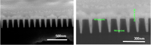
Copper interconnects metallization of Si wafer
Developed by CAE.
Potentiostatic regulation of features filling on Si wafers
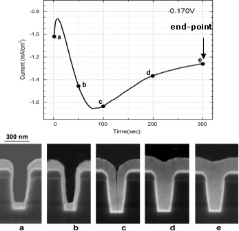
Potentiostatic regulation of features filling over copper seed layer on Si wafers. Selective copper filling of wafer features is carried out at the potentiostatic mode with regulation on the plating process. Accurate control of features filling (end-point) is provided by a current-time profile of copper plating in a solution containing organic additives.
Top: Current-Time profile of copper filling features at a potential of -170 mV (vs SCE).
Bottom: FIB cross-sections taken subsequently at copper filling after: (a) 0s, copper seed (b)50s (c)100s (d)200s (e)300s.
Seedless Copper interconnect (IC) metallization
A novel method of seedless copper interconnect metallization of futures smaller than 32nm over TaN/Ta barrier.
The method includes 2 steps:
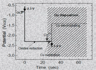
a) removing of Ta oxide from the Ta barrier by the electrochemical reduction of Ta oxide.
b) prevent re-oxidation of Ta barrier by copper plating in the invariable electrochemical bath.
Seedless Cu plating on Ta from an a Alkaline activated bath
Seedless Cu filling over TaN/Ta features commercial wafer (22 nm trenches)